A Moulded Interconnect Device (MID) is a single construction unit, that consists of circuit traces embedded onto moulded thermoplastics to form electrical pathways and landings for surface mount components. Compared to 2-dimensional printed circuit boards or a flexible circuit wrap, MID technology offers a greater freedom of design and a miniaturization of electronic components (by reducing the number of required parts). As a result, weight and fitting space can be effectively reduced.
LPKF LDS Technology ProcessOne of the predominantly used manufacturing methods is laser direct structuring (LDS). The process is based on laser structuring and electroless metallization to create metallic circuits and traces on moulded thermoplastic components. The company LPKF - the LDS method developer - shows the process steps. The production line shown below is used to make a fully functioning digital thermometer as a 3D-MID. The 3D-MID production line was set up at "SMT Hybrid Packaging 2012" in Nuremburg.
1. Step 3D-MID: Layout Production
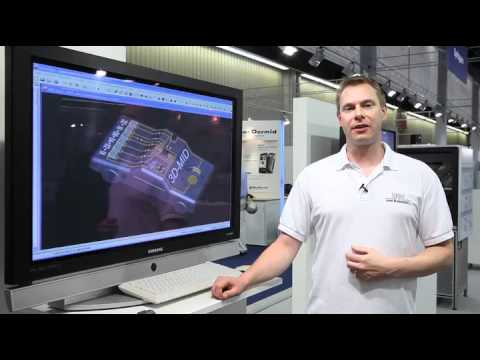
2. Step 3D-MID: Injection Molding
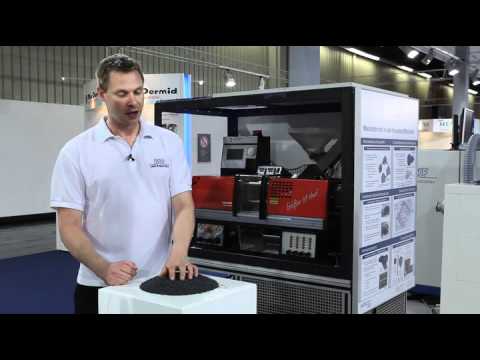
3. Step 3D-MID: Laser Structuring
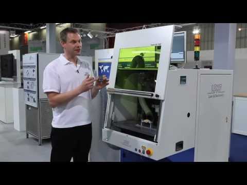
4. Step 3D-MID: Metallization
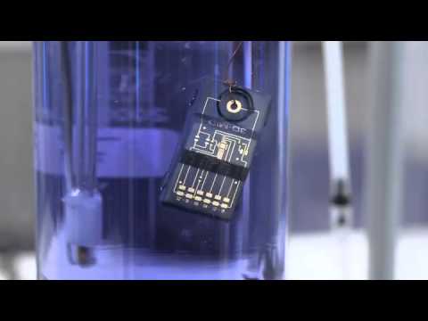
5. Step 3D-MID: Assembly
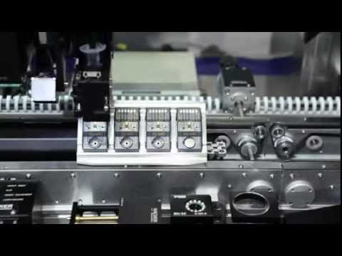
6. Step 3D-MID: Soldering

Comments